Information is an important ingredient in decision making, for applications, and in basic research. As science and technology advance, it is crucial to collect, process and transmit information in real time. This eventually allows us to improve decision making, and perhaps even modify the collection of the type of information, in a dynamical fashion i.e. adding feedback. In some sense, this task is akin to the development of an “artificial skin” which is sensitive to a variety (“integral”) of different stimuli in close physical proximity (“nano”). This proposal deals with key issues that relate to all aspects of this important task and is a first step in the development of an integrated supersensor.
Useful information must
have the following characteristics: a) integral, i.e. as many different
type of stimuli as possible, b) acquired in close physical proximity,
c) preprocessed and d) transmitted to a remote location for further more
sophisticated processing. In order to acquire information which is useful
for military applications, sensors must have the following additional
requirements; increased packing density, enhanced sensitivity, radiation
hardness, high speed, small dissipation, integration, remote programming,
tribology, corrosion, stealth and reduced cost. This is a formidable task
which requires the collaboration of scientists from the different disciplines
of physics, chemistry, materials science, and engineering. Moreover in
order to ground these studies in reality, contributions by the consumers
(i.e. military users) are crucial.

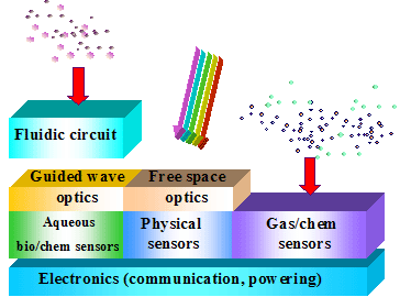
Fig. 1 Conceptual Design of Integrated Nanostructured Supersensors.
We envision that this MURI will be a first step toward the development
of a supersensor that is sensitive to different types of stimuli (magnetic,
optical, chemical and biological), will allow local limited preprocessing
and decision making and will transmit this data to a remote location.
The MURI will address some of the key issues related to this formidable
task including; developing, miniaturizing and improving the sensitivity
of different nanosensors and integrating them into a single chip together
with power supplies and data processing devices. A number of basic research
issues arise on the road toward this goal and will be addressed here.
These include controlling interfaces between dissimilar materials, improving
the sensitivity of individual sensors, transfer and wafer bonding of dissimilar
sensors and materials, and subjecting different sensors to a variety of
environments. In addition to the development of individual sensors, this
proposal will stress the integration of these into a single device. Because
of the optimization of different sensors requires radically different
conditions (substrates, growth methods, temperature,…), integration
will be performed by slicing and moving them (once they are prepared)
to the final chip. We envision that there will be a number of issues of
compatibility, electrical, chemical and physical interaction, programming,
etc issues which will have to be addressed as they arise. The development
of an integral nanosensor would also have many nonmilitary applications
in disparate fields such as process monitoring, environmental, robotics,
and probably others not yet envisioned.
To make this task a success, we have assembled a lean group that consists of experts with proven records in integration, magnetic, infrared, chemical and biological sensors, and miniaturization. The participants are chemistry, physics, and engineering faculty members from UCSD together with researchers from the Air Force Research Laboratory at Wright-Patterson Air Force Base (AFRL-WPAFB) and the U.S. Army Soldier and Biochemical Command (SBCCOM) Laboratories. It is crucial to realize that in addition to solving several specific research problems, this MURI will fulfill an important educational objective: namely to educate young investigators in this field. This will be done by intimately involving graduate students and postdocs in the research problems to be addressed. In addition, we will have graduate students and postdocs specifically assigned to work at the partner Defense labs. They will become familiar with state of the art facilities available there and with the specific needs the end users have. In order to assure that proper progress is made, an external advisory committee will be named to evaluate and advise the MURI director.
Statement of the Problem
In order to focus the problem, it is crucial to specify the final aim more precisely. We envision that the integral supersensor to be developed under this proposal will be aimed toward detecting a massive moving object which emits infrared radiation and produces a variety of chemical and biological outputs. Since it is impossible to have all sensors operational all the time, a logical hierarchy will be developed to trigger one sensor based on the response from others. To conserve power and decrease cost, nanostructuring and overall integration on a single chip will be investigated. We expect that in the future these types of sensors will be self-powered, miniaturized and massively deployable. More specifically, we will aim toward integrating all sensors on Si substrates, although this aim may have to be revised depending on the results obtained during the initial stages of research.
The general
aims of this project are to: a) develop a set of sensors in different
areas which have high sensitivity, small size and low power consumption,
b) integrate them on a single chip, studying all the critical issues which
may arise from this task, c) develop the logic, hierarchy and software
for powering the various sensors and d) develop concepts for transmission
of the data to a remote location. Since this is a daunting task, a number
of unknown problems may arise, which requires some flexibility in readjusting
the goals as the research is carried out.

